Dear Marziyeh,
I come a bit late to the party with just a few general physical comments for your consideration.
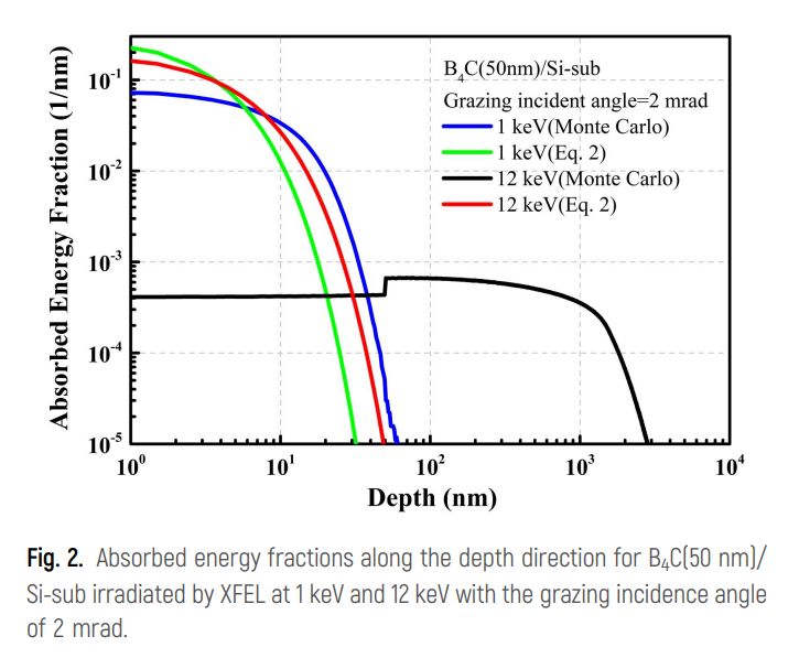
Then for nanometer thickness, the results are not accurate and it does not depend on Fluka, it is for all Monte Carlo simulations, right?
If I follow correctly, you have 1-12 keV photons impinging on a 50 nm slab of B4C or Ru on a Si substrate and want to examine energy deposition in this geometry.
Your incoming photons will be absorbed and emit photoelectrons (along with fluorescence gammas and Auger electrons as the inner-shell vacancy relaxes), which will deposit energy as they propagate in the geometry, being eventually stopped in the “depths” of the several-micron-thick Si substrate. All of these interaction mechanisms are accounted for if you pass a DEFAULTS card with PRECISIOn as suggested above.
The produced 1-12 keV photoelectrons propagating in the slab+substrate will deposit energy in two complementary (and carefully consistent) ways:
- Energy losses larger than 1 keV will lead to the production and explicit transport of a secondary electron (delta ray), thanks to your
EMFCUT card with electron production/transport thresholds down to 1 keV.
- Smaller losses are deposited along the electron step as per FLUKA’s ionization model, relying on a stopping power calculation with energy-loss fluctuations applied on top.
Underpinning this scheme (adopted in various flavors by basically all general-purpose MC codes) is the adoption of an ionization model for charged particles in a material, derived under the assumption that the material is “infinite”, homogeneous, and isotropic. The problem is that when you try to resolve things at the few nm scale, there are aspects in the energy loss of low-energy electrons (which ultimately govern energy deposition problems) near solid interfaces which deviate significantly from the conventional “bulk material” picture.
The energy loss of electrons below ~5 keV in the first few nm near the boundary between two solids is subject to a series of interesting physical effects. For instance, there are energy loss features confined to the first couple nm within the surface (excitation of surface plasmons), considerably changing the energy-loss picture one has from homogeneous and isotropic media as ordinarily adopted in general-purpose codes. To address these local details in the first few nm near solid interfaces, one needs detailed optical response functions of the solid material at either side, and a non-negligible amount of computation to eventually obtain an “energy loss function” that depends on the distance to the interface, the direction of motion (surprising differences exist depending on whether the electron goes in or out), the energy, etc., as per Figs 6 and 8 of https://analyticalsciencejournals.onlinelibrary.wiley.com/doi/epdf/10.1002/sia.5175.
On the other hand, both electrons and photons sufficiently below 1 keV start to feel details the electronic structure / local binding environment of the target atom/molecule/crystal, with direct impact on both the differential cross section for elastic scattering of electrons and the absorption of low-energy photons…
As you can see, the huge amount of highly case-specific information one needs to rigorously address these details, and the possibly diverging CPU time involved, make them necessarily fall out of scope general-purpose codes (including here FLUKA, PENELOPE, and others).
As a side remark, various codes will track electrons down to different energies: 1 keV for FLUKA, 100 eV or so for PENELOPE (the developers of the latter are exquisitely careful to stress that for e- below 1 keV simulation results should be taken as a semi-quantitative guess). In any case, they won’t account for the aspects addressed above, which become increasingly relevant the lower you go in energy and the smaller you go in scale towards the nm.
While being well aware of these formal considerations, one then turns to practical life. Overall, one may still employ general-purpose codes for a semi-quantitative assessment of energy deposition in geometries a mere few nm or tens of nm thick, but being well aware that if one pushes too much, one eventually risks missing relevant physical details.
“Too long, didn’t read” version: one may (ab)use general-purpose MC codes for low-energy electron transport problems in geometries some nm thick, but it would be wise to exercise caution and take the result as no more than a semi-quantitative assessment.
Cheers,
Cesc